Microchip Production Machines Explained: Types, Processes, and Advanced Technology
Microchips are tiny electronic components that form the foundation of modern digital systems. They are used in smartphones, computers, vehicles, industrial controllers, medical electronics, communication equipment, data centers, and many other technologies.
Microchip production machines are specialized systems used to transform semiconductor materials into highly precise integrated circuits. The manufacturing process involves multiple stages, including wafer preparation, photolithography, deposition, etching, ion implantation, inspection, packaging, and testing.
The semiconductor manufacturing process exists because modern electronic devices require components that can process information quickly while using very little physical space. A single semiconductor wafer can contain many individual chips, with each chip containing millions or billions of microscopic electronic structures.
Modern semiconductor equipment must operate with extremely high precision. Even a small particle or manufacturing variation can affect a chip's performance. For this reason, semiconductor fabrication plants use controlled environments, advanced measurement systems, automation, and sophisticated process-control technologies.
The broader microchip manufacturing equipment market includes machines for front-end wafer fabrication as well as back-end assembly and semiconductor testing. Each machine performs a specific function within a carefully controlled production sequence.
Why Microchip Production Machines Matter Today
The growing dependence on electronics has increased the importance of advanced semiconductor manufacturing. Industries such as automotive technology, artificial intelligence, telecommunications, renewable energy, industrial automation, and consumer electronics all depend on semiconductor components.
One important reason microchip production machines matter is precision. Semiconductor manufacturing works at extremely small dimensions, so conventional manufacturing methods are not sufficient for many advanced chip structures.
These machines also help manufacturers maintain consistency across large numbers of wafers. Automated process controls can monitor temperature, pressure, chemical conditions, alignment, dimensions, and other parameters during production.
Key areas influenced by semiconductor manufacturing include:
- Artificial intelligence and high-performance computing
- Smartphones, tablets, and personal computers
- Electric and connected vehicles
- Industrial automation and robotics
- Telecommunications infrastructure
- Medical and diagnostic electronics
- Internet of Things devices
- Renewable-energy power electronics
- Aerospace and defense electronics
- Data centers and cloud computing infrastructure
The semiconductor industry also has a major role in technological resilience. Recent disruptions have shown how dependence on limited manufacturing capacity can affect electronics supply chains.
Advanced semiconductor equipment therefore supports not only chip production but also broader technology development and manufacturing capacity.
Major Types of Microchip Production Machines
Microchip manufacturing requires a large collection of specialized equipment. Different machines are used at different stages of the production cycle.
Wafer Processing Equipment
Wafer processing machines prepare semiconductor wafers for subsequent manufacturing steps. Silicon is commonly used as the substrate, although other semiconductor materials are important for particular applications.
Wafer preparation can involve cleaning, polishing, surface treatment, and measurement. High-quality wafer surfaces are essential because microscopic defects can affect later fabrication stages.
Photolithography Machines
Photolithography equipment transfers circuit patterns onto semiconductor wafers. A photosensitive material called photoresist is applied to the wafer before exposure.
Advanced lithography systems use extremely precise optical technologies to create increasingly small circuit patterns. Extreme ultraviolet, or EUV, lithography is particularly important for some advanced semiconductor manufacturing processes.
Lithography is one of the most technically demanding stages because pattern placement and dimensional accuracy directly affect chip performance.
Deposition Equipment
Deposition machines place extremely thin layers of materials onto the wafer surface. Different deposition techniques are selected according to the required material and structure.
Common approaches include:
- Chemical vapor deposition
- Physical vapor deposition
- Atomic layer deposition
- Other specialized thin-film techniques
These layers can form insulating, conducting, or semiconductor structures within the chip.
Etching Machines
Etching equipment removes selected portions of material from the wafer. This creates the shapes and structures required by the circuit design.
Etching may be performed using chemical or plasma-based processes. Advanced semiconductor manufacturing requires highly controlled etching because excessive or uneven material removal can damage microscopic structures.
Ion Implantation Systems
Ion implantation equipment introduces selected impurities into semiconductor materials. This process modifies electrical properties in specific areas of the wafer.
Precise control of ion energy, dose, and placement is important for creating semiconductor devices with the desired electrical characteristics.
Cleaning Equipment
Cleaning systems remove particles, residues, and unwanted materials between manufacturing stages.
Cleanliness is critical because semiconductor structures are extremely small. A particle that appears insignificant to the human eye can become a major defect at the chip scale.
Inspection and Metrology Equipment
Inspection machines identify physical defects, while metrology equipment measures dimensions and process characteristics.
These systems may use optical inspection, electron-beam techniques, imaging systems, and other measurement technologies.
Process monitoring allows manufacturers to identify variations before they affect a larger production batch.
Semiconductor Packaging and Testing Equipment
After wafer fabrication, individual dies are separated and prepared for packaging. Packaging protects the chip and provides connections between the semiconductor device and the surrounding electronic system.
Testing equipment evaluates electrical and functional characteristics. Advanced packaging technologies are becoming increasingly important as chip designs become more complex.
The Microchip Manufacturing Process Explained
Semiconductor fabrication follows a sequence of highly controlled steps rather than one single manufacturing operation.
A simplified process includes:
- Silicon wafer preparation
- Wafer cleaning
- Thin-film deposition
- Photoresist coating
- Photolithography
- Etching
- Ion implantation
- Repeated layering and patterning
- Inspection and measurement
- Wafer testing
- Dicing
- Packaging
- Final testing
Many of these stages are repeated numerous times. The exact sequence varies according to chip architecture, semiconductor material, manufacturing technology, and application.
Advanced semiconductor fabrication can involve hundreds of individual process steps. Automated equipment and process-control systems help maintain consistency throughout the production cycle.
Recent Semiconductor Technology Developments
The semiconductor industry has continued to evolve rapidly during 2025 and 2026. Several trends are influencing microchip production machines and manufacturing strategies.
Smaller and More Complex Chip Structures
Advanced semiconductor manufacturing continues to move toward smaller process technologies. Smaller structures can enable greater transistor density, although they also create increasingly demanding requirements for lithography, deposition, etching, inspection, and process control.
Growth of Advanced Packaging
Advanced packaging has become a major area of semiconductor development. Techniques such as chiplets, 2.5D integration, 3D integration, and high-bandwidth connections can combine multiple semiconductor components within sophisticated packages.
This trend is increasing the importance of back-end manufacturing equipment alongside traditional wafer fabrication systems.
AI Semiconductor Demand
The rapid expansion of artificial intelligence applications has increased interest in high-performance computing chips, memory technologies, advanced packaging, and semiconductor manufacturing capacity.
This development is influencing equipment requirements across fabrication, inspection, testing, and packaging.
Greater Manufacturing Automation
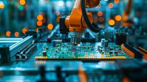
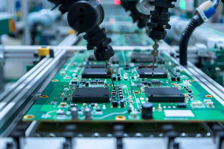
Factories are increasingly integrating robotics, machine vision, automated material handling, digital process monitoring, and data analytics.
Automation can help coordinate complex manufacturing steps and improve process visibility. It also supports cleaner and more controlled production environments.
Regional Semiconductor Investment
During 2025 and 2026, governments and semiconductor companies continued developing domestic and regional semiconductor manufacturing capabilities. These initiatives are intended to strengthen technology ecosystems and reduce vulnerabilities in critical electronics supply chains.
Semiconductor Laws, Policies, and Government Programs
Semiconductor manufacturing is influenced by industrial policy, export controls, environmental regulations, workplace requirements, and technology-development programs.
In the United States, the CHIPS and Science Act remains an important framework supporting domestic semiconductor manufacturing and research.
The European Union has also developed the European Chips Act, which aims to strengthen semiconductor capabilities across Europe.
India has introduced the India Semiconductor Mission and related initiatives to encourage semiconductor manufacturing, packaging, design, and ecosystem development.
Other countries and regions have introduced their own semiconductor strategies. Policies can address areas such as:
- Semiconductor fabrication capacity
- Research and development
- Advanced packaging
- Workforce development
- Supply-chain resilience
- Export controls
- Environmental management
- Strategic technology investment
Companies involved in semiconductor manufacturing must also comply with applicable environmental, chemical-handling, occupational-safety, and electronic-waste requirements in their operating regions.
Because policies can change, manufacturers and researchers should consult current government regulations when making compliance decisions.
Tools and Resources for Learning About Microchip Manufacturing
People studying semiconductor production can use a variety of educational and technical resources.
Helpful resources include:
- Semiconductor process-flow diagrams
- Wafer fabrication learning modules
- Lithography simulation tools
- Semiconductor device calculators
- Basic transistor-design software
- Process-control templates
- Cleanroom technology guides
- Semiconductor materials references
- Manufacturing terminology glossaries
- University-level semiconductor courses
- Government semiconductor policy portals
- Technical research databases
- Equipment maintenance documentation
- Semiconductor packaging guides
For beginners, starting with wafer fabrication fundamentals, semiconductor materials, transistor operation, and basic process-flow concepts can make advanced manufacturing technologies easier to understand.
Frequently Asked Questions About Microchip Production Machines
What machines are used to manufacture microchips?
Microchip manufacturing uses many types of equipment, including lithography systems, deposition equipment, etching machines, ion implantation systems, cleaning equipment, inspection tools, metrology systems, packaging equipment, and semiconductor testing machines.
Why is photolithography important in chip manufacturing?
Photolithography transfers extremely detailed circuit patterns onto semiconductor wafers. It is a central process because the accuracy of these patterns affects the structure and performance of the resulting chip.
What materials are commonly used in microchip manufacturing?
Silicon is the most widely used semiconductor material for many integrated circuits. Other materials, including silicon carbide and gallium nitride, are also important for specific applications such as power electronics and high-frequency technologies.
How does automation help semiconductor manufacturing?
Automation helps coordinate complex production steps, monitor process conditions, move materials, collect manufacturing data, and identify potential variations. It can improve consistency and process visibility when properly implemented.
Why is advanced packaging becoming important?
Advanced packaging allows multiple semiconductor components to work together in compact configurations. Chiplets, 2.5D designs, and 3D integration can support higher system-level performance and help address challenges associated with increasingly complex chip designs.
Conclusion
Microchip production machines are essential to modern semiconductor manufacturing. From wafer preparation and photolithography to deposition, etching, inspection, packaging, and testing, each equipment category performs an important role in creating reliable semiconductor devices.