Semiconductor Manufacturing Equipment: Technology, Processes & Industry Trends
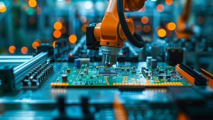
Semiconductor manufacturing equipment refers to the specialized machinery and systems used to produce integrated circuits, memory devices, sensors, power semiconductors, and other electronic components. These machines support nearly every stage of chip production, from preparing silicon wafers to depositing materials, creating microscopic patterns, inspecting structures, assembling devices, and testing finished components.
Modern semiconductor manufacturing depends on extremely precise processes. A tiny defect can affect the performance or reliability of a chip, so production environments require controlled temperatures, clean air, advanced measurement systems, and highly accurate equipment.
The manufacturing process generally begins with a silicon wafer. Equipment gradually builds and modifies layers on the wafer through processes such as deposition, lithography, etching, ion implantation, cleaning, and inspection. After the wafer has been processed, additional equipment supports dicing, packaging, and electrical testing.
The growing use of artificial intelligence, cloud computing, smartphones, electric vehicles, industrial automation, and connected devices has increased attention toward semiconductor production. As chip architectures become more sophisticated, manufacturers are also adopting more advanced semiconductor equipment.
Why Semiconductor Equipment Matters Today
Semiconductor manufacturing equipment plays an important role in the global electronics ecosystem. Chip manufacturers depend on specialized equipment to achieve the accuracy, consistency, and production volumes required by modern electronics.
One major factor is the growing demand for computing power. Artificial intelligence applications require processors and memory technologies capable of handling large amounts of data. This has increased investment in leading-edge logic, advanced memory, high-bandwidth memory, and advanced packaging.
Equipment is also important for manufacturers producing mature-node semiconductors. Automotive electronics, industrial controllers, power management devices, medical electronics, communication equipment, and many other applications continue to use established semiconductor technologies.
Key areas affected by semiconductor equipment include:
- Artificial intelligence and high-performance computing
- Data centers and cloud infrastructure
- Automotive electronics and electric vehicles
- Industrial automation and robotics
- Consumer electronics
- Telecommunications and networking
- Renewable energy and power management
- Medical and scientific electronics
The equipment market is also closely connected with semiconductor supply-chain resilience. Governments and manufacturers in several regions are expanding domestic production capabilities to reduce dependence on concentrated supply networks.
According to SEMI, global semiconductor manufacturing equipment sales were forecast in July 2026 to reach $165.9 billion in 2026, representing a 23.2% year-over-year increase. The organization linked the expansion to AI infrastructure, leading-edge logic, advanced memory, and back-end technologies.
Major Types of Semiconductor Manufacturing Equipment
Semiconductor production involves many equipment categories. Each machine performs a specific function within the manufacturing flow.
Wafer Processing Equipment
Wafer processing equipment modifies the surface and structure of semiconductor wafers. Common processes include deposition, etching, cleaning, oxidation, and ion implantation.
These systems must maintain extremely precise process conditions because semiconductor structures can be measured at microscopic or nanometer scales.
Lithography Equipment
Lithography equipment transfers circuit patterns onto a wafer coated with photosensitive material. It is one of the most important steps in semiconductor manufacturing because it defines many of the structures used to create electronic circuits.
Advanced lithography has become increasingly important as manufacturers develop smaller and more complex semiconductor architectures.
Deposition Equipment
Deposition systems place extremely thin layers of materials onto wafers. Depending on the application, manufacturers may use chemical vapor deposition, physical vapor deposition, atomic layer deposition, or related techniques.
Layer thickness and uniformity are closely monitored because small variations can influence semiconductor performance.
Etching Equipment
Etching removes selected materials from a wafer to create the desired structures. Both wet and dry etching techniques are used across semiconductor manufacturing.
Advanced plasma-based etching is particularly important for producing complex three-dimensional structures.
Inspection and Metrology Equipment
Inspection systems identify defects, while metrology equipment measures dimensions and process characteristics.
These technologies support process control by helping manufacturers identify problems before they affect large quantities of wafers.
Assembly, Packaging, and Test Equipment
After wafer processing, semiconductor devices undergo cutting, assembly, packaging, and electrical testing.
Advanced packaging has become increasingly important because modern chip performance is influenced not only by transistor scaling but also by how multiple dies, memory components, and interconnects are integrated.
Semiconductor Manufacturing Process Overview
A simplified semiconductor production flow can be viewed as a sequence of connected stages.
| Manufacturing Stage | Typical Equipment | Main Purpose |
|---|---|---|
| Wafer preparation | Cleaning and surface systems | Prepare wafer surfaces |
| Deposition | Thin-film deposition systems | Add material layers |
| Lithography | Patterning equipment | Create circuit patterns |
| Etching | Plasma or wet etching systems | Remove selected materials |
| Implantation | Ion implantation equipment | Modify electrical properties |
| Inspection | Optical and measurement systems | Detect defects and variations |
| Packaging | Assembly and packaging equipment | Protect and connect devices |
| Testing | Semiconductor test systems | Verify electrical performance |
The stages are repeated many times for complex chips. Process control therefore becomes essential throughout production.
Recent Semiconductor Equipment Trends
The semiconductor equipment industry has changed rapidly during 2025 and 2026. Artificial intelligence is one of the strongest drivers of current investment.
In June 2026, SEMI reported that global semiconductor equipment billings reached $36.55 billion in the first quarter of 2026, up 14% from the same period a year earlier. The organization identified AI-related investment in leading-edge logic, DRAM, and advanced packaging as important contributors.
Advanced packaging is another major trend. As conventional scaling becomes more complex, manufacturers are increasingly combining multiple dies and technologies within sophisticated packages.
High-bandwidth memory is also influencing equipment requirements. AI accelerators require fast access to large volumes of data, increasing interest in advanced memory manufacturing and packaging technologies.
Smart manufacturing is developing alongside these technologies. SEMI highlighted AI-driven manufacturing and advanced packaging as major themes in July 2026, reflecting the industry's shift toward greater automation, data analysis, and system-level integration.
The 300mm wafer segment is another important area. SEMI reported in October 2025 that global 300mm fab equipment spending was expected to total $374 billion from 2026 through 2028, supported by AI chip demand and regional semiconductor manufacturing expansion.
Important Technology Trends
- AI-assisted semiconductor manufacturing
- Advanced lithography
- Gate-all-around transistor architectures
- High-bandwidth memory production
- Advanced semiconductor packaging
- Chiplet-based architectures
- Automated inspection and metrology
- Digital twins and process simulation
- Factory data analytics
- Greater manufacturing automation
These trends indicate that semiconductor manufacturing is moving toward more integrated, automated, and data-driven production environments.
Laws, Policies, and Government Programs
Semiconductor manufacturing is influenced by industrial policy, environmental requirements, export controls, workplace regulations, and technology development programs.
In India, the India Semiconductor Mission coordinates major initiatives designed to develop a semiconductor and display ecosystem. Its programs cover semiconductor fabs, display manufacturing, compound semiconductors, silicon photonics, sensors, semiconductor packaging, and chip design.
The Design Linked Incentive framework also supports semiconductor design development and aims to strengthen India's domestic chip-design ecosystem.
Another important development was India's Electronics Component Manufacturing Scheme, approved by the Union Cabinet on March 28, 2025, and notified on April 8, 2025. The program is intended to strengthen the electronics component manufacturing ecosystem and integrate domestic capabilities with global value chains.
Environmental and operational requirements are also relevant. Semiconductor facilities must manage chemicals, gases, wastewater, emissions, energy consumption, and hazardous materials according to applicable national and regional rules.
Because semiconductor technologies are strategically important, international trade and export-control regulations can also affect access to advanced equipment and manufacturing technologies. These rules can change, so manufacturers must monitor applicable government notifications and regulatory updates.
Tools and Resources for Understanding Semiconductor Manufacturing
Several resources can help students, engineers, researchers, manufacturers, and general readers understand semiconductor equipment and production.
Useful resources include:
- Semiconductor process-flow diagrams
- Wafer fabrication simulation tools
- Lithography and etching learning modules
- Semiconductor device simulators
- Statistical process-control templates
- Yield-analysis spreadsheets
- Cleanroom monitoring dashboards
- Equipment maintenance records
- Process-control charts
- Semiconductor technology databases
- Industry market reports
- Government semiconductor policy portals
- Engineering textbooks and technical training materials
For beginners, process-flow diagrams are particularly useful because they show how individual manufacturing steps connect to one another.
For technical teams, statistical process control, defect-density analysis, equipment utilization data, and yield calculations can provide deeper insight into manufacturing performance.
Frequently Asked Questions
What is semiconductor manufacturing equipment?
Semiconductor manufacturing equipment consists of specialized machines used to fabricate, inspect, package, and test semiconductor devices. Major categories include lithography, deposition, etching, cleaning, inspection, metrology, packaging, and testing systems.
Why is semiconductor equipment important for AI chips?
AI chips require advanced logic, memory, interconnects, and packaging technologies. Semiconductor equipment enables manufacturers to create the complex structures and high-density components needed for these applications.
What is advanced semiconductor packaging?
Advanced packaging refers to technologies that integrate semiconductor dies, memory, interconnects, and other components in sophisticated configurations. It can improve system performance, bandwidth, and integration without relying only on transistor scaling.
What role does India play in semiconductor manufacturing?
India is developing semiconductor manufacturing and design capabilities through programs coordinated by the India Semiconductor Mission. Government initiatives cover areas including semiconductor fabs, packaging, compound semiconductors, sensors, and chip design.
What are the major semiconductor manufacturing trends in 2026?
Major trends include AI-driven equipment investment, advanced memory, high-bandwidth memory, advanced packaging, smart manufacturing, automated inspection, leading-edge logic, and regional semiconductor supply-chain development.
Conclusion
Semiconductor manufacturing equipment forms the technological foundation of modern chip production. From wafer preparation and lithography to inspection, packaging, and testing, every stage depends on specialized equipment capable of maintaining extremely precise process conditions.